TSMC: We Have Working CFET Transistors in the Lab, But They Are Generations Away
by Anton Shilov on May 25, 2023 8:00 AM EST- Posted in
- Semiconductors
- TSMC
- CFET
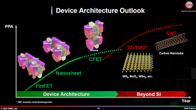
Offering an update on its work with complementary field-effect transistors (CFETs) as part of the company's European Technology Symposium 2023, TSMC has revealed that it has working CFETs within its labs. But even with the progress TSMC has made so far, the technology is still in its early days, generations away from mass production. In the meantime, ahead of CFETs will come gate-all-around (GAA) transistors, which TSMC will be introducing with its TSMC's upcoming N2 (2nm-class) production nodes.
One of TSMC's long-term bets as the eventual successor to GAAFETs, CFETs are expected to offer advantages over GAAFETs and FinFETs when it comes to power efficiency, performance, and transistor density. However, these potential benefits are theoretical and dependent on overcoming significant technical challenges in fabrication and design. In particular, CFETs are projected to require the usage of extremely precise lithography (think High NA EUV tools) to integrate both n-type and p-type FETs into a single device, as well as determining the most ideal materials to ensure appropriate electronic properties.
Just like other chip fabs, TSMC is working on a variety of transistor design types, so having CFETs working in the lab is important. But it's also not something that is completely unexpected; researchers elsewhere have previously assembled CFETs, so now it's up to industry-focused TSMC to figure out how to bring about mass production. To that end, TSMC is stressing that CFETs are not in the near future.
"Let me make a clarification on that roadmap, everything beyond the nanosheet is something we will put on our [roadmap] to tell you there is still future out there," said Kevin Zhang, senior vice president at responsible for technology roadmap, business strategy. "We will continue to work on different options. I also have the add on to the one-dimensional material-[based transistors] […], all of those are being researched on being investigated on the future potential candidates right now, we will not tell you exactly the transistor architecture will be beyond the nanosheet."
Indeed, research projects take a long time and when you are running many of them in parallel, you never know which of them comes to fruition. Even at that point, it is hard to tell which of potential structure candidates TSMC (or any other fabs) will choose, Ultimately, fabs have to meet the needs of their larger customers (e.g., Apple, AMD, MediaTek, Nvidia, Qualcomm) at the time when this production node is ready for high volume manufacturing.
To that end, TSMC is going to use GAA structures for years to come, according to Zhang.
"Nanosheet is starting at 2nm, it is reasonable to project and that nanosheet will be used for at least a couple of generations, right," asked Zhang rhetorically. "So, if you think about CFETs, we've leveraged [FinFETs] for five generations, which is more than 10 years. Maybe [device structure] is somebody else's problem to worry, then you can continue to write a story."
Source; TSMC European Technology Symposium 2023


3 Comments
View All Comments
del42sa - Friday, May 26, 2023 - link
a reaction to this : https://www.tomshardware.com/news/intel-shows-new-...https://www.imec-int.com/en/articles/imec-puts-com...
CHADBOGA - Friday, May 26, 2023 - link
If the forum mods could unban me that would be good. I have served my time.Santoval - Saturday, May 27, 2023 - link
"Nanosheet is starting at 2nm, it is reasonable to project and that nanosheet will be used for at least a couple of generations, right,"Just a couple of generations of GAAFETs?!
No, no way. I doubt CFETs will be made commercially available before the early 2030s.