TSMC: Ecosystem for 2nm Chip Development Is Nearing Completion
by Anton Shilov on October 12, 2023 5:00 PM EST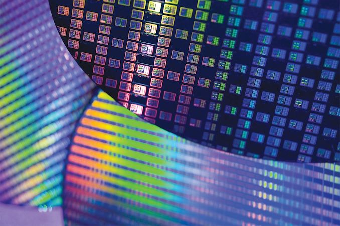
Speaking to partners last week as part of their annual Open Innovation Platform forum in Europe, a big portion of TSMC's roadshow was dedicated to the next generation of the company's foundry technology. TSMC's 2 nm-class N2, N2P, and N2X process technologies are set to introduce multiple innovations, including nanosheet gate-all-around (GAA) transistors, backside power delivery, and super-high-performance metal-insulator-metal (SHPMIM) capacitor over the next few years. But in order to take advantage of these innovations, TSMC warns, chip designers will need to use all-new electronic design automation (EDA), simulation, and verification tools as well as IP. And while making such a big shift is never an easy task, TSMC is bringing some good news to chip designers early-on: even with N2 still a couple of years out, many of the major EDA tools, verification tools, foundation IP, and even analog IP for N2 are already available for use.
"For N2 we could be working with them two years in advance already because nanosheet is different," said Dan Kochpatcharin, Head of Design Infrastructure Management at TSMC, at the OIP 2023 conference in Amsterdam. "[EDA] tools have to be ready, so what the OIP did is to work with them early. We have a huge engineering team to work with the EDA partners, IP partners, [and other] partners."
| Advertised PPA Improvements of New Process Technologies Data announced during conference calls, events, press briefings and press releases |
|||||
| TSMC | |||||
| N5 vs N7 |
N3 vs N5 |
N3E vs N5 |
N2 vs N3E |
||
| Power | -30% | -25-30% | -34% | -25-30% | |
| Performance | +15% | +10-15% | +18% | +10-15% | |
| Chip Density* | ? | ? | ~1.3X | >1.15X | |
| Volume Manufacturing |
Q2 2022 | H2 2022 | Q2/Q3 2023 | H2 2025 | |
*Chip density published by TSMC reflects 'mixed' chip density consisting of 50% logic, 30% SRAM, and 20% analog.
Preparations for the start of N2 chip production, scheduled for sometime in the second half of 2025, began long ago. Nanosheet GAA transistors behave differently than familiar FinFETs, so EDA and other tool and IP makers had to build their products from scratch. This is where TSMC's Open Innovation Platform (OIP) demonstrated its prowess and enabled TSMC's partners to start working on their products well in advance.
By now, major EDA tools from Cadence and Synopsys as well as many tools from Ansys and Siemens EDA have been certified by TSMC, so chip developers can already use them to design chips. Also, EDA software programs from Cadence and Synopsys are ready for analog design migration. Furthermore, Cadence's EDA tools already support N2P's backside power delivery network.
With pre-built IP designs, things are taking a bit longer. TSMC's foundation libraries and IP, including standard cells, GPIO/ESD, PLL, SRAM, and ROM are ready both for mobile and high-performance computing applications. Meanwhile, some PLLs exist in pre-silicon development kits, whereas others are silicon proven. Finally, blocks such as non-volatile memory, interface IP, and even chiplet IP are not yet available - bottlenecking some chip designs - but these blocks in active development or planned for development by companies like Alphawave, Cadence, Credo, eMemory, GUC, and Synopsys, according to a TSMC slide. Ultimately, the ecosystem of tools and libraries for designing 2 nm chips is coming together, but it's not all there quite yet.
"[Developing IP featuring nanosheet transistors] is not harder, but it does take more cycle time, cycle time is a bit longer," said Kochpatcharin. "Some of these IP vendors also need to be trained [because] it is just different. To go from planar [transistor] to FinFET, is not harder, you just need to know how to do the FinFET. [It is] same thing, you just need to know how to do [this]. So, it does take some to be trained, but [when you are trained], it is easy. So that is why we started early."
Although many of the major building blocks for chips are N2-ready, a lot of work still has to be done by many companies before TSMC's 2 nm-class process technologies go into mass production. Large companies, which tend to design (or co-design) IP and development tools themselves are already working on their 2 nm chips, and should be ready with their products by the time mass production starts in 2H 2025. Other players can also fire up their design engines because 2 nm preps are well underway at TSMC and its partners.


20 Comments
View All Comments
my_wing - Thursday, October 12, 2023 - link
There isn't discrimination here but please list the vendor that will use TSMC N2 before 2027.Apple, Intel, nVidia, AMD, Qualcomm, MediaTek, Samsung, Amazon, Google, Microsoft, (smaller one from now on) Lockhead Martin, Ericsson, Nokia (But OpenRAN is current 90%+ held by Intel),
This is more a paper launch then anything.
I am now laughing those in MLID that saying Intel Arrow Lake is moving to TSMC N3E, now with this information, it is proven that GAA and FinFET is totally different, how is Arrow Lake design on GAA + Backside Power Delivery can fit back to FinFET. Arrow Lake Lion Cove is different to Redwood Cove, this prove that MLID is fake news media with no connection to Intel Staff. Just milling idea inside his bedroom without the internet.
This also shows that why Qualcomm did not go with Intel 18A, because the cost of redesign is too much.
If this is the case, I think it will not before (or just before) 2030 that Infineon, Renesa, TI, Broadcom to start using TSMC N2 / Intel 18A / Samsung 3nm, until EUV High-NA got a good depreciation by the high end application, meaning that even initial GAA is build by Intel and Samsung using non High-NA machine, there might be a need to move to High-NA to reduce cost.
TekCheck - Friday, October 13, 2023 - link
Even Intel does not know always what process or specs they are going to end up with on different lines of products and they change it on-the-go, for example they marketed 192 EUs (VEs now) on Meteor Lake iGPU and ended up on 128 EUs. In addition, initial 320 EUs (VEs now) on Arrow Lake became 192 EUs. So, Tom from MLID is fed by whatever current information is available. This information sometimes changes. It's not written in stone like 10 Commandments. Also, not everyone in Intel knows what's going on on all fronts. That's impossible.my_wing - Friday, October 13, 2023 - link
Sorry your comment make no sense, I am talking about the CPU that MLID was talking about, now you move to ARC/GPU, if you look at SemiAccurate, you understand that iGPU tile actually held back by TSMC, we know way ahead (at least in 2022 Q1) that intel can't be using TSMC N3 on GPU, it was likely that when Meteor Lake is plan that it will be the case and it might be in TSMC N3B, but the more into the development, the more unlikely that TSMC will met it's deadline show Intel will stay with TSMC N5/N6.Yes not written in stone like 10 Commandments, but anyone with a brain will know that TSMC N3E without GAA+PowerVia will not be able to move (backward) to FinFET, there is no way Intel will make this investment, is not 10 Commandments but it is the rules of Economic, So it is just as strong, except the 10 Commandments is from God. So MLID is Fake news media with no connection to Intel Staff directly working with CPU. Else no one even a junior intern will think that arrow lake CPU title will be made by TSMC.
Dante Verizon - Saturday, October 14, 2023 - link
If TSMC doesn't succeed, Intel won't come close to achieving it in processes below 3nm.Flunk - Monday, October 16, 2023 - link
I don't know what you're expecting, these new process announcements are not really for consumers. TSMC announces this stuff to stir up interest from their customers, who will build on the process and then announce their new chips. Those new chips will then get integrated into products and then those product-makers will announce those.For a consumer perspective any TSMC announcement is going to be a "paper launch". So I'm not sure why you're seemingly surprised by this.
do_not_arrest - Monday, October 16, 2023 - link
Not sure you know what you are talking about. Moving a die from one technology to another does not have the implications you think ("can fit back to FinFet"). That's not the way it works. You don't fit anything back to anything else. Intel would simply design a new CPU chiplet on another technology. In this case the reports are that some of the cores change from Redwood->Lion and Crest->Sky. The WHOLE idea of 3D die stacking and segregating the die into basic functional blocks is to allow this kind of modularity when designing a system.melgross - Friday, October 13, 2023 - link
If the future follows the past, I would imagine that Apple would be the first vendor to use the technology. If it’s true that TSMC is on track to have mass production 2H 2025, as they say, then certainly 2027 is very likely, even if they get pushed back by a quarter or two.Doug_S - Friday, October 13, 2023 - link
Yes unless TSMC's N2 rollout is seriously delayed Apple will be using N2 for iPhone 18 in 2026. If they could somehow pull that H2 date forward to Q2 Apple would be able to use it for iPhone 17, but I'm gonna assume "H2" means December like it did for N3 meaning iPhone 17 gets N3P.my_wing - Sunday, October 15, 2023 - link
I have serious doubt about this, be honestly, if you know Chinese, you can watch some finance youtube talk bashing USA that Taiwan can build and USA can't they are flexible la la la. Be very honest, the flip side of the coin is that Taiwanese builder will request work to move on else will go online and blame TSMC for delay and this is what they did, and of course TSMC will go out there is silent it in a CCP fashion. This is what they did and try to claim down things.Then you see Intel mentioned ASML will received High-NA in Dec 2023, as TSMC and ASML relationship is very good, we can assume that TSMC will get High-NA no later than April 2024, then TSMC will use High-NA for N2, look at how difficult TSMC achieve N3B (rumor but too many of them to be ignored), the best bet for TSMC to have a reasonable N2 is through High-NA.
This is not the same story for Intel, remember PowerVIA, that meant that Intel M0 is going to be simpler than TSMC N2 as cables runs from the back.
Whether TSMC will delay or not depends on ASML, and you know ASML delay history.
Because TSMC can't even make me feels like they can make N3B properly, i.e. rumors, iPhone 15 Pro Max Pan Fry Egg, introducing N3E, how am I going to have confidence that multi patterning on EUV works in TSMC. So the best bet is TSMC wait for high na then move to N2.
Whether 2027 is very likely, it can be just as easy to say 2027 is very unlikely, and move to 2028 is more likely, then Intel will be what 4 years ahead because 20A is TSMC N2P not TSMC N2.
Doug_S - Sunday, October 15, 2023 - link
I think you don't understand how much work goes into rolling out a new process if you think receiving their first high NA scanner in early 2024 would allow them to use it for N2.First of all they need way more than one for mass production at their scale, second of all they have already frozen N2's characteristics. They have the fab space built out and exactly planned where every piece of hardware goes - there is no room for the far larger high NA scanners, no power budget for them, and nothing in N2's specs that requires them.
Maybe they will slot in high NA scanners 2-3 years down the road when the N2 family has reached the end of the line and is on its final long life iteration, like N6 was for the N7 family.
But other than that - which won't concern Apple or others who following the leading edge train - high NA will be reserved whatever they call the "N1.4" node that comes after N2 late this decade.