Intel's Xeon E5-2600 V2: 12-core Ivy Bridge EP for Servers
by Johan De Gelas on September 17, 2013 12:00 AM EST
The core architecture inside the latest Xeon is typically a step behind what you find inside the latest desktop and notebook chips. A longer and more thorough validation is one reason, but there is more. The high-end model of the Xeon E5-2600 V2 or "Ivy Bridge EP" is, aside from the core architecture, completely different from the Ivy-bridge "i7 \-3xxx" that was launched in the spring of last year. With up to twelve cores, two integrated memory controllers, no GPU and 30MB L3 cache, it is the big brother of the recently reviewed Ivy-bridge E (Core i7-4960X). Intel has three die flavors of the Ivy-bridge EP:
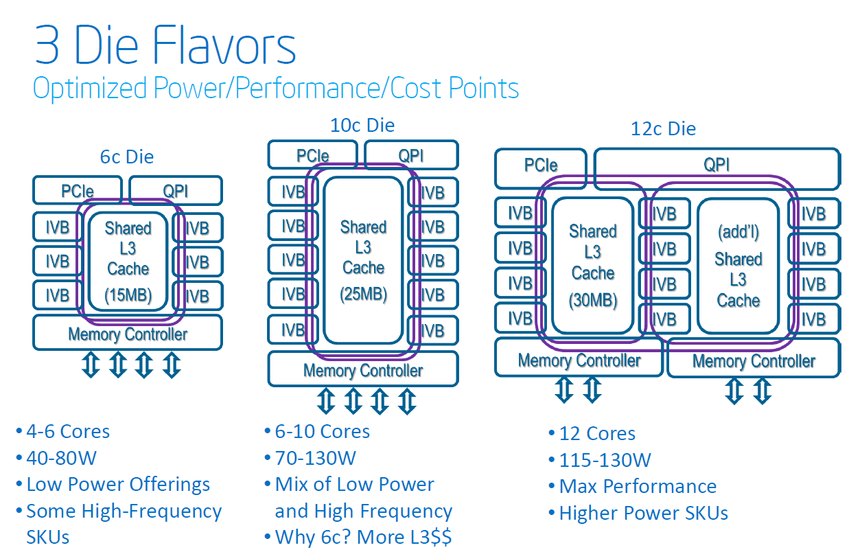
The first one is the one with the lowest core count (4/6 cores), which is found in SKUs targeted at the workstation and enthusiast market (high frequencies) or low power SKUs; this is the core being used in the enthusiast Ivy Bridge-E processors. The second one is targeted at the typical server environment with higher core counts (6 to 10 cores) and a larger L3 cache (25MB). The third and last one is the high performance HPC and server die, with 12 cores, two memory controllers for lower memory latency, and 30MB of L3 cache.
The cool thing about the newest Xeon E5 processors is that they run on the same Romley EP platform as LGA-2011 chips. This should save the OEMs a lot of time and money, and hopefully these savings will trickled down to the customers. Let's see how Intel's latest server update performs, and if it manages to impress more than the enthusiast Ivy Bridge-E.


70 Comments
View All Comments
Kevin G - Tuesday, September 17, 2013 - link
Odd that Intel went the 3 die route with Ivy Bridge-EP. It was no surprise that the lowend would be a variant of the 6 core Ivy Bridge-E found in the Core i7-4900 series. Apple leaked that the line up would scale to 12 cores. The surprise is a native 10 core part and the differences between it and the 12 core design.Judging from the diagrams, Intel altered its internal ring bus for connecting cores. One ring goes orbits around all three columns of cores while another connects two columns. Thus the cores in the middle column have better latency for coherency as they have fewer stops on the ring bus to reach any core. The outer columns should have similar latency than the native 10 core chip for coherency: fewer cores to stop but longer traces on the die between columns.
Not disclosed is how the 12 core chip divides cache. Previously each core would have a 2.5 MB of L3 cache that was more local than the rest of the L3 cache. The middle column may have access to L3 cache on both sides.
The usage of dual memory controllers on the 12 core die is interesting. I wonder what measurable differences it produces. I'd fathom tests with a mix of reads/writes (ie databases) would show the greatest benefit as a concurrent read and write may occur. In a single socket configuration, enabling NUMA may produce a benefit. (Actually, how many single socket 2011 boards have this option?)
madmilk - Tuesday, September 17, 2013 - link
It looks like each ring is connected to two columns. One ring goes around all three, but does not connect to the center column.JlHADJOE - Tuesday, September 17, 2013 - link
I'm guessing the 12-core might see action in the 8P segment, which is well overdue for an update.psyq321 - Tuesday, September 17, 2013 - link
There will be 15-core E7 8xxx v2 CPUs based on the same IvyTown architecture.As Intel is not showing the die-shot of a 12 core Ivy EP, I wonder if the 15-core EX and 12-core EP are using the same 3x5 die.
Kevin G - Tuesday, September 17, 2013 - link
The memory controller interfaces are different between the Ivy Bridge-EP and Ivy Bridge-EX. The EP uses DDR3 in all of its forms (vanilla, ECC, buffered ECC, LR ECC) where as the EX version is going to use a serial interface similar in concept to FB-DIMMs. There will be two types of memory buffers for the EX line, one for DDR3 and later another that will use DDR4 memory. No changes need to be made to the new EX socket to support both types of memory.Brutalizer - Tuesday, September 17, 2013 - link
I would have expected this newest Intel 12-core cpu to perform better. For instance, in Java SPECjbb2013 benchmarks, it gets 35,500 and 4,500. However, the Oracle SPARC T5 gets 75.700 and 23.300 which totally demolishes the x86 cpu. Have not the x86 cpus improved that much in comparison to SPARC? The x86 still lags behind?https://blogs.oracle.com/BestPerf/entry/20130326_s...
JohanAnandtech - Tuesday, September 17, 2013 - link
Be careful when you compare inflated, for marketing purposes results with independent "limited optimization" results ;-)Phil_Oracle - Friday, February 21, 2014 - link
What do you mean by inflated for marketing purposes? SPECjbb2013 is clearly a real world, recent benchmark that’s full audited by all vendors on the SPEC committee. If you make such claims, surely you have some evidence?extide - Tuesday, September 17, 2013 - link
Dont forget those T5's run at TDP's in the 200-300W range... If you clocked up one of these babies to those power levels I am sure it would be >= to the T5.Kevin G - Tuesday, September 17, 2013 - link
TDP's are indeed higher on the SPARC side but not as radically as you indicate. Generally they do not consume more than 200W. (Unfortunately Oracle doesn't give a flat power consumption figure for just the CPU, this is just an estimate based upon their total system power calculator. For reference, the POWER7 is 200W and the POWER7+ is 180W.)