A Closer Look at Broadwell & its New Small Form Factor Package
by Anand Lal Shimpi on September 11, 2013 9:53 PM EST- Posted in
- CPUs
- Intel
- Trade Shows
- IDF 2013
- Broadwell
First, a quick recap. There are four different Haswell versions: D, M, ULT and ULX. D is for desktop, M is for mobile, ULT is for Ultrabooks and ULX is for low power tablet designs. The latter carries the Y-series branding.
Broadwell, the 14nm successor to Haswell, will likely be available in similar flavors (there's still some uncertainty on whether or not we'll see a desktop Broadwell though). Earlier today Intel flashed a Broadwell sample up on stage at IDF and I noticed its smaller package compared to the single chip Haswell solution. I managed to get some hands on time with the Broadwell chip that was shown off.
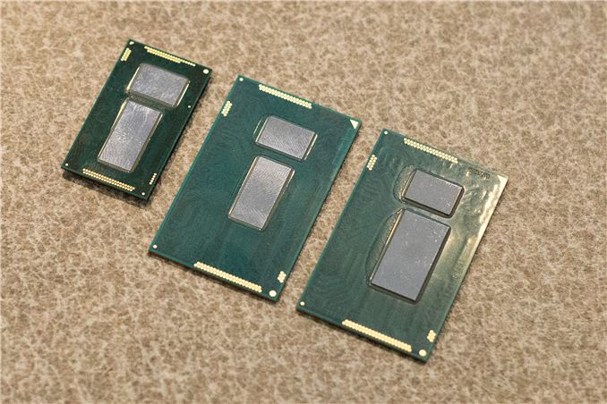
Broadwell is pin compatible with Haswell. In the pic above (and below) the two chips on the right are pin compatible Broadwell and Haswell ULT samples. The chip on the left however is a newer, smaller form factor version. This smaller package will only be offered for Broadwell ULX (Y-series) parts.
 From left to right: Broadwell SFF, Broadwell ULT/ULX and Haswell ULT/ULX
Given that Broadwell will likely usher in a new era of hybrid tablet/notebook devices, I expect this smaller package was built at the request of one or more large OEMs looking to offer a premium tablet/2-in-1 option but were put off by the board area requirements of Haswell ULX vs. a traditional ARM solution. By the looks of it, this smaller Broadwell still won't be quite as small as what you can presently get from the ARM camp but it's probably a very useful update.
I'm running between meetings now - but anyone want to use the photos here and our Haswell die area info to come up with an estimate for Broadwell SFF package size and Broadwell die size? :)


18 Comments
View All Comments
UltraWide - Wednesday, September 11, 2013 - link
We need something to determine scale, the chips look huge just from the pics. hahasolipsism - Wednesday, September 11, 2013 - link
I concur.mikk - Wednesday, September 11, 2013 - link
The Broadwell Die is 63,4% the size of the Haswell Die in this photo. If anyone knows the package size from Haswell-Y it would help.Goty - Wednesday, September 11, 2013 - link
That is remarkably close to the numbers I just posted below. Hooray for me not screwing up!Goty - Wednesday, September 11, 2013 - link
A very rough Photoshop estimate puts the Broadwell CPU die at 114 mm^2 and the package at 590 mm^2.mikk - Wednesday, September 11, 2013 - link
The package size from Haswell-U/Y is 40x24 mm big according to the datasheet. I did a new calculation. I got for the Haswell die 126 mm² and for the Broadwell die 80 mm². It is apparently a 2+2 die.MrSpadge - Thursday, September 12, 2013 - link
Looks like we'll soon need diamond heatspreaders to keep these bad boys cool!FieryUP - Thursday, September 12, 2013 - link
Package size is 40x24mm for Haswell-ULT and 30x16.5mm for Broadwell-ULX. Based on the latter data, it may be easier to calculate the die size for Broadwell-ULX.mikk - Thursday, September 12, 2013 - link
The Broadwell die size from the smaller package is the same. Based on your 30x16.5mm size from the smaller package I measured 81 mm² for Broadwell.Goty - Thursday, September 12, 2013 - link
Are you sure you're measuring the right thing? The onboard eDRAM (i.e. Crystalwell, the top chip on all three packages) is 84 mm^2, so the CPU can't be so small.