EUV
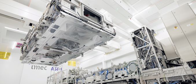
Imec and ASML have announced that the two companies have printed the first logic and DRAM patterns using ASML's experimental Twinscan EXE:5000 EUV lithography tool, the industry's first High-NA EUV scanner. The lithography system achieved resolution that is good enough for 1.4nm-class process technology with just one exposure, which confirms the capabilities of the system and that development of the High-NA ecosystem remains on-track for use in commercial chip production later this decade. "The results confirm the long-predicted resolution capability of High NA EUV lithography, targeting sub 20nm pitch metal layers in one single exposure," said Luc Van den hove, president and CEO of imec. "High NA EUV will therefore be highly instrumental to continue the dimensional scaling of logic and memory technologies, one of...
Samsung Foundry: 2nm Silicon in 2025
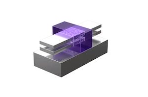
One of the key semiconductor technologies beyond 3D FinFET transistors are Gate-All-Around transistors, which show promise to help extend the ability to drive processors and components to higher performance...
29 by Dr. Ian Cutress on 10/6/2021
Samsung Foundry to Almost Double Output by 2026
It’s hard not to notice that we’re in the middle of a semiconductor crunch right now. Factories are running at full steam, but pinch points in the supply chain...
6 by Dr. Ian Cutress on 10/6/2021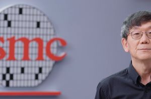
An AnandTech Interview with TSMC: Dr. Kevin Zhang and Dr. Maria Marced
In the past week, TSMC ran its 2021 Technology Symposium, covering its latest developments in process node technology designed to improve the performance, costs, and capabilities for its customers...
18 by Dr. Ian Cutress on 6/8/2021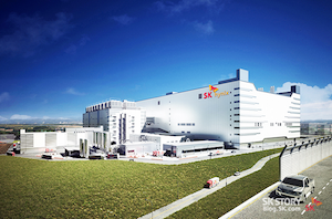
SK Hynix to Build $106 Billion Fab Cluster: 800,000 Wafer Starts a Month
Capping off a busy week for fab-related news, South Korea authorities this week gave SK Hynix a green light to build a new, 120 trillion won ($106.35 billion) fab...
41 by Anton Shilov on 4/2/2021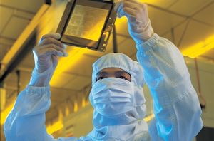
EUV Pellicles Ready For Fabs, Expected to Boost Chip Yields and Sizes
Foundries started limited usage of extreme ultraviolet (EUV) lithography for high-volume manufacturing (HVM) of chips in 2019. At the time, ASML's Twinscan NXE scanners were good enough for production...
35 by Anton Shilov on 3/31/2021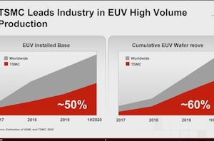
TSMC: We have 50% of All EUV Installations, 60% Wafer Capacity
One of the overriding central messages to TSMC’s Technology Symposium this week is that the company is a world leader in semiconductor manufacturing, especially at the leading edge process...
32 by Dr. Ian Cutress on 8/27/2020
‘Better Yield on 5nm than 7nm’: TSMC Update on Defect Rates for N5
One of the key metrics on how well a semiconductor process is developing is looking at its quantitative chip yield – or rather, its defect density. A manufacturing process...
107 by Dr. Ian Cutress on 8/25/2020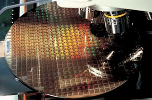
TSMC Details 3nm Process Technology: Full Node Scaling for 2H22 Volume Production
At TSMC’s annual Technology Symposium, the Taiwanese semiconductor manufacturer detailed characteristics of its future 3nm process node as well as laying out a roadmap for 5nm successors in the...
58 by Andrei Frumusanu on 8/24/2020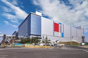
Samsung to Produce DDR5 in 2021 (with EUV)
Samsung is on track to start volume production of DDR5 and LPDDR5 memory next year using a manufacturing technology that will take advantage of extreme ultraviolet lithography (EUVL). In...
20 by Anton Shilov on 3/25/2020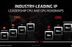
AMD Clarifies Comments on 7nm / 7nm+ for Future Products: EUV Not Specified
As part of AMD’s Financial Analyst Day 2020, the company gave the latest updates for its CPU and GPU roadmap. A lot of this we have seen before, with...
37 by Dr. Ian Cutress on 3/5/2020
TSMC & Broadcom Develop 1,700 mm2 CoWoS Interposer: 2X Larger Than Reticles
With transistor shrinks slowing and demand for HPC gear growing, as of late there has been an increased interest in chip solutions larger than the reticle size of a...
18 by Anton Shilov on 3/4/2020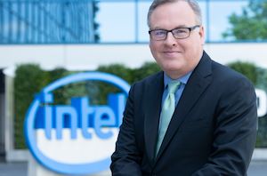
Intel CFO: Our 10nm Will Be Less Profitable than 22nm [Morgan Stanley Transcription]
This week at Morgan Stanley’s Analyst Conference, Intel’s CFO, George Davis, sat down to discuss the future of where Intel’s profitability lies. No stranger to the odd comments relating...
92 by Dr. Ian Cutress on 3/4/2020
Samsung Starts Mass Production at V1: A Dedicated EUV Fab for 7nm, 6nm, 5nm, 4nm, 3nm Nodes
Samsung Foundry has started mass production of chips using its 6LPP and 7LPP manufacturing processes at its new V1 fab. The new facility employs one of the industry’s first...
30 by Anton Shilov on 2/20/2020
ASML Ramps Up EUV Scanners Production: 35 in 2020, Up to 50 in 2021
ASML shipped 26 extreme ultraviolet lithography (EUVL) step-and-scan systems to its customers last year, and the company plans to increase shipments to around 35 in 2020. And the ramp-up...
22 by Anton Shilov on 1/23/2020
TSMC Boosts CapEx by $1 Billion, Expects N5 Node to Be Major Success
TSMC is on track to begin high-volume production of chips using its 5 nm technology in the coming months, the company said in its conference call last week. While...
40 by Anton Shilov on 1/22/2020
Intel Hires Fab Veteran, Former GlobalFoundries CTO Dr. Gary Patton
Intel has hired Dr. Gary Patton, the former CTO at GlobalFoundries and an ex-head of IBM Microelectronics business. Dr Patton was leading Global Foundries leading edge processes before that...
21 by Anton Shilov on 12/11/2019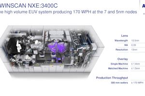
EUV Wafers Processed and TwinScan Machine Uptime: A Quick Look
One of the interesting elements that came out of some of our discussions at the IEDM conference this year revolve around the present deployment of EUV. Currently only one...
29 by Dr. Ian Cutress on 12/11/2019
TSMC: 5nm on Track for Q2 2020 HVM, Will Ramp Faster Than 7nm
TSMC’s 5 nm (N5) manufacturing technology is projected to provide significant benefits when it comes to performance, power, and area scaling, which is why the contract maker of semiconductors...
27 by Anton Shilov on 10/23/2019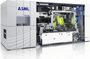
EUV Demand is Up: EUV Device Manufacturer ASML Beats Sales Estimates
Between the smartphone revolution, cloud computing, and the Internet of Things, the demand for cutting-edge chips has never been higher. And if you have any doubts about that, then...
46 by Anton Shilov on 10/16/2019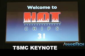
Hot Chips 31 Keynote Day 2: Dr. Phillip Wong, VP Research at TSMC (1:45pm PT)
The keynote for the second day is from TSMC, with Dr. Phillip Wong taking the stage to talk about the latest developments in TSMC's research and portfolio. The talk...
12 by Dr. Ian Cutress on 8/20/2019


